
Technical Insight
DGU Separation for Semiconducting and Metallic SWCNT
Density-gradient ultracentrifugation separates Single-Walled Carbon Nanotubes (SWCNT) fractions by surfactant-assisted density contrast, allowing semiconducting, metallic, and purified SWCNT grade routes to be screened with electronic-type, spectra, purity, dispersion, and device evidence.
Author: Aurexene Materials Engineering Team · Last updated: 2026-08-28
Quick Answer
DGU separation is useful when the project must choose between semiconducting SWCNT, metallic SWCNT, and high-purity unseparated SWCNT. Use the separated grade as an identity and screening route, then prove the final film, device, contact, optical, or sensor response with matched application evidence.
Problem
Single-wall carbon nanotube feedstock can contain both semiconducting and metallic fractions. The wrong fraction can make a transistor fail to switch, a transparent conductor miss its resistance target, or a sensor drift for reasons that look like a material problem but are actually electronic-type, contact, residue, or dispersion problems.
Mechanism
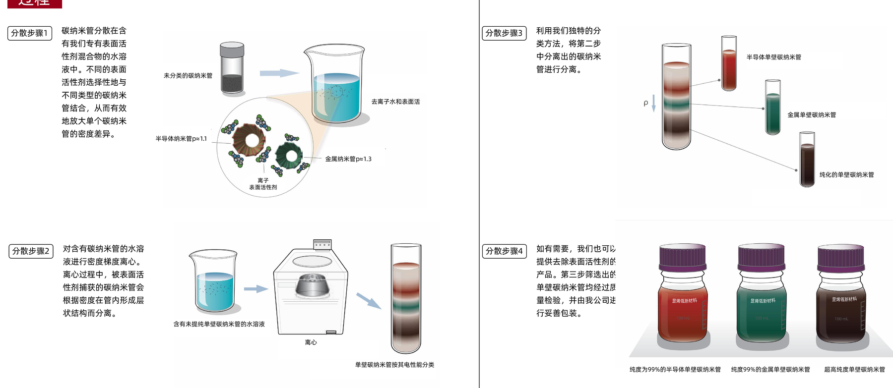
The brochure describes density-gradient ultracentrifugation as a surfactant-assisted separation route. SWCNT is dispersed in an aqueous system, different nanotube types acquire different effective densities, centrifugation forms separated bands, and the fractions are collected as semiconducting, metallic, or purified SWCNT products.
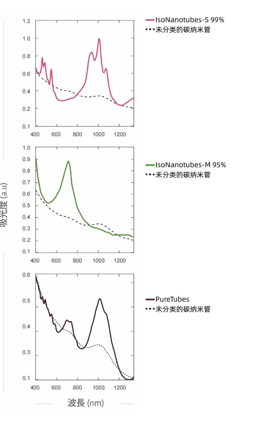
Absorption spectra are useful identity evidence because separated semiconducting and metallic fractions show different optical responses. They are not a finished-film or finished-device guarantee.
Tradeoff
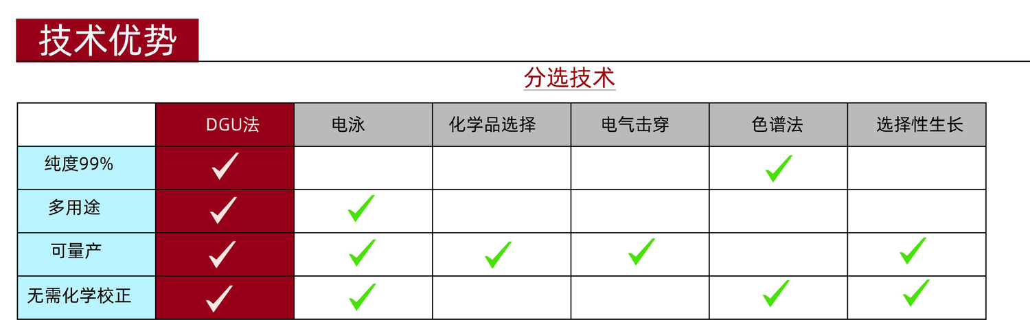
DGU can create clearer semiconducting and metallic grade routes, but it also makes grade choice, surfactant state, dispersion medium, document state, contact design, and aging evidence more important. The value is highest when electronic type changes the engineering decision.
Material Strategy
| Grade route | Brochure identity | Use when | First evidence gate |
|---|---|---|---|
| IsoNanotubes-S | Semiconducting SWCNT; brochure reports 1.2-1.7 nm diameter, 300 nm to 4 um length, catalyst impurity below 1%, amorphous carbon impurity 1-5%, and 90%, 95%, 98%, or 99% purity options. | Transistor, switch, optoelectronic, or sensor concepts require semiconducting behavior. | Electronic type, absorption spectra, contact resistance, channel geometry, hysteresis, and aging. |
| IsoNanotubes-M | Metallic SWCNT; brochure reports 1.2-1.7 nm diameter, 300 nm to 4 um length, catalyst impurity below 1%, amorphous carbon impurity 1-5%, and 70%, 95%, 98%, or 99% purity options. | Transparent conductor, flexible conductor, electrothermal film, or conductive-network screening requires metallic network behavior. | Sheet resistance, transmission, haze, residue, adhesion, bend retention, and humidity aging. |
| PureTubes | High-purity unseparated SWCNT; brochure reports the same diameter and length band with catalyst impurity below 1% and amorphous carbon impurity 1-5%. | A control or early network screen is needed before separated electronic type is justified. | Dispersion stability, spectra, network uniformity, resistance, and process retention. |
Recommended Architectures
| Route | Related application | Validation priority |
|---|---|---|
| Semiconducting SWCNT channel or sensor film | SWCNT grade review | Electronic type, contacts, on/off or sensor response, baseline drift, humidity, and aging. |
| Metallic SWCNT transparent conductor | Transparent Conductive Films, Coatings & Fibers | Sheet resistance, transmission, haze, flexibility, adhesion, residue, and environmental retention. |
| Conductive or electrothermal network | Photothermal & Electrothermal Systems | Resistance map, heating uniformity, voltage/current/power, film quality, cycling, and hot-spot risk. |
Application Map
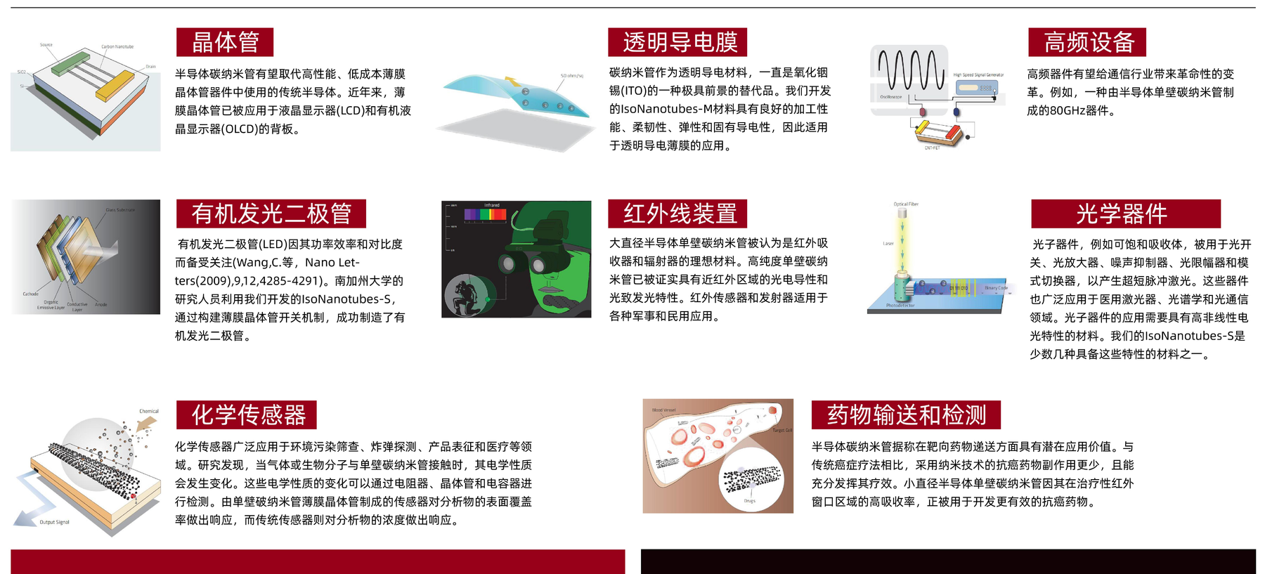
The brochure names CNT transistors, transparent conductive films, OLED routes, high-frequency devices, infrared devices, optical devices, chemical sensors, and drug-delivery/detection concepts. In the public content graph, transparent conductor and electrothermal questions route to existing application pages; transistor, optical-device, infrared, and sensor mentions remain SWCNT grade-validation context until verified application-specific evidence exists. Biomedical or therapeutic claims stay research-only until approved safety and regulatory evidence exists.
Measurement & Validation
- Freeze the selected grade, purity option, surfactant state, dispersion medium, storage condition, and document status.
- Record absorption spectra or electronic-type evidence for the selected fraction and compare it only against matched dispersion or film states.
- For devices, separate contact resistance from channel or film response and report geometry, substrate, contact metal, passivation, and process history.
- For transparent or electrothermal films, measure sheet resistance, transmission, haze, adhesion, residue, bend retention, humidity, and cycling on the same film stack.
- For sensors, prove analyte response, selectivity, baseline drift, humidity cross-sensitivity, recovery, and repeatability.
Related Products
Related Applications
- Transparent Conductive Films, Coatings & Fibers
- Photothermal & Electrothermal Systems
- Printed Electronics Inks & Conductive Pastes
Downloads & Engineering Support
The brochure is approval-required as a public download. Request current grade documents before using any value as a purchase, device, or public specification.
Need to apply this boundary to a grade, formulation, test method, or production route? Discuss it with the Aurexene Materials Engineering Team.