
Application
Electronic Packaging & Interconnects
Screen conductive adhesives, die-attach and printed-conductor routes, and electrically insulating thermal fillers for contact resistance, reliability, and process-compatible electronic packaging integration.
Quick Answer
Screen silver-, copper-, or nickel-filled conductive adhesives and pastes alongside CNT/graphene-metal hybrid formulation candidates. Treat every hybrid as an unqualified formulation family until final-joint data confirm contact resistance, corrosion, migration, thermal cycling, adhesion, and process compatibility. Use Hexagonal Boron Nitride (hBN)/AlN ceramic filler systems only for thermal paths that must remain electrically insulating.
What Are Electronic Packaging & Interconnects?
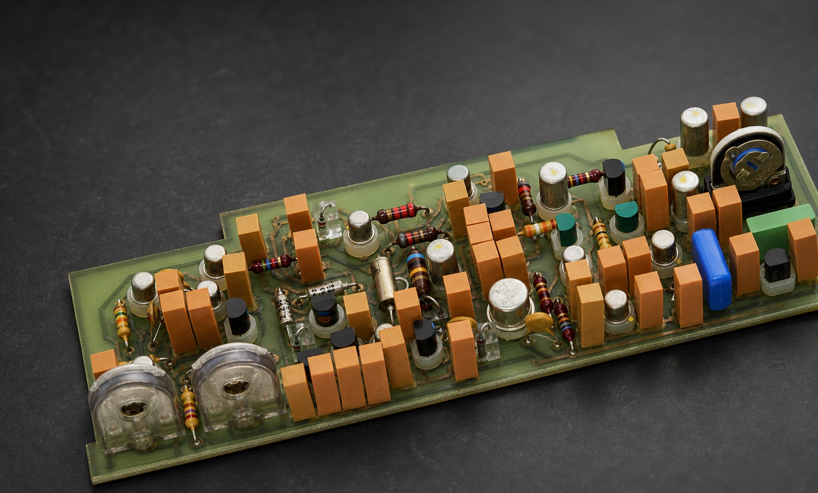
Electronic packaging and interconnect systems need stable electrical contact, thermal-cycling reliability, CTE compatibility, controlled corrosion or migration risk, and process-compatible conductive pathways.
Mechanism
Conductive fillers, sintered particles, or metal-carbon networks create conductive pathways and may reduce bulk or contact resistance only when network continuity, filler dispersion, metal-carbon contact quality, oxide control, and interface cleanliness are validated in the final joint geometry. The useful mechanism is continuity retained across the real joint while thermal cycling, moisture, ionic residue, and voltage bias act on adhesion, contact area, corrosion, and metal migration.
The mechanism depends on the following system interfaces:
- substrate and metallization surface state
- joint, line, coating, or bondline geometry
- filler dispersion, oxide control, residue, and interface cleanliness
- binder, cure or sintering profile, pressure, and atmosphere
- current density, voltage bias, humidity, thermal cycling, and service temperature
Material Selection
Read each row as a scenario-specific route: the guidance explains why a material fits, while the rejection boundary shows when to stop screening it.
| Scenario | Materials | Guidance |
|---|---|---|
| Diamond-filled insulating package-layer formulation study | AX-DND | Treat AX-DND only as an evaluation-stage filler in a defined TIM, underfill, encapsulant, or molding compound. Qualify the finished layer and complete package-to-cold-plate path; do not infer package suitability from powder identity. |
| Silver-filled conductive adhesive, die-attach, or paste | Silver powder or silver-filled paste family | Screen when low contact resistance and process temperature justify a silver route, then qualify electrochemical migration, leakage, corrosion, adhesion, and aged resistance in the final geometry. |
| Copper-filled conductive adhesive, contact, or printed conductor | Copper powder or copper-filled paste family | Screen when copper-compatible processing is available and oxide, corrosion, galvanic, humidity-bias, residue, and migration risks can be controlled. |
| Nickel-filled conductive system | Nickel powder or nickel-filled formulation family | Screen only when nickel surface chemistry, oxidation, magnetic behavior, contact stability, and the required resistance window can be qualified against the final package. |
| Metal-nanocarbon hybrid formulation | CNT/graphene-metal hybrid formulation family | Treat as a formulation candidate rather than an automatically improved contact solution; require matched controls and final-joint evidence for dispersion, interface formation, resistance, and aging. |
| Electrically insulating thermal path | hBN/AlN ceramic filler system | Screen only when heat spreading or interface thermal resistance must improve while dielectric isolation is preserved; reject it for current-carrying joints or contact-resistance reduction. |
Scope Boundary
- This is not packaging material in the shipping or enclosure sense; it concerns electrical, thermal, and bonded connections within electronic assemblies.
- Do not use this route for structural packaging alone when no electrical, thermal, or bonded interconnect function is required.
Scenarios and Subtypes
Use the host-system or subtype constraint to narrow the material direction before comparing grades or supplier data.
| Scenario | Key constraint | Material direction |
|---|---|---|
| Diamond-filled TIM, underfill, encapsulant, or molding-compound study | Exact grade, aggregate state, surface chemistry, ionic purity, loading, flow, cure, voids, dielectric behavior, CTE, modulus, adhesion, moisture, warpage, thermal cycling, and package-level heat path. | AX-DND as a conditional formulation-development filler only. |
| Conductive interconnect path | Contact resistance, conductive continuity, corrosion or migration, and processing temperature. | Silver-, copper-, or nickel-filled adhesives and pastes, selected by joint function, process window, and reliability evidence. |
| Printed or coated conductor | Sheet or line resistance, coating continuity, adhesion, rheology, cure/sintering temperature, and humidity/bias reliability. | Silver- or copper-filled pastes, nickel-filled systems, or evidence-backed carbon/metal formulation families selected by geometry, resistance method, metal risk, and process window. |
| Conductive adhesive or contact interface | Contact resistance drift, compression or bondline geometry, adhesion, thermal cycling, electrochemical migration, and flux or residue exposure. | Choose the metal-filled adhesive family only after silver, copper, or nickel surface and migration risks are matched to the complete substrate and metallization stack. |
| Electrically insulating thermal interface | Thermal resistance, dielectric strength, leakage current, filler loading, viscosity, interface pressure, and thermal-cycle stability. | hBN/AlN ceramic filler systems, not metal-filled or metal-nanocarbon conductive routes. |
Target Performance Bands
Interpret each target together with its stated unit, condition, geometry, and validation method; no single value selects a material route by itself.
| Target type | Reference band | Note |
|---|---|---|
| Static contact or bonded-joint resistance | Report mΩ or Ω using a four-wire/Kelvin method, with current, contact pressure, joint area, metallization, and initial-versus-aged state. | ASTM B539 defines contact-resistance measurement techniques but leaves acceptance limits application-specific. |
| Printed or coated conductor resistance | Report line resistance in Ω or sheet resistance in Ω/sq with conductor length, width, dry thickness, substrate, cure or sintering profile, and electrode geometry. | Do not compare line, sheet, bulk, and contact resistance without retaining the applicable geometry and test method. |
| Insulation resistance between biased conductors | Report SIR in Ω with conductor spacing, applied bias, temperature, humidity, residue state, and exposure duration. | Use the customer-specified IPC or equivalent method and pair SIR results with ECM inspection where metal migration is a credible failure mechanism. |
Failure Modes
Use failure rows to identify a measurable trigger and the corresponding design response.
| Failure type | Root cause | Manifestation | Mitigation strategy |
|---|---|---|---|
| Contact resistance drift | Oxide growth, incomplete interparticle contact, cure or sintering variation, interface fatigue, or geometry-dependent current constriction. | Four-wire/Kelvin resistance rises or becomes intermittent after aging, humidity exposure, or thermal cycling, with matching cross-section or interface evidence. | Validate resistance mapping before and after humidity, thermal cycling, and aging exposure. |
| Corrosion or migration | Moisture, ionic residue, applied bias, incompatible metallization, or insufficient corrosion and migration control. | Leakage current, SIR decline, dendritic growth, corrosion products, migration paths, or localized resistance change after exposure. | Screen metal-containing candidates with method-conditioned humidity-bias exposure, resistance monitoring, and microscopy. |
Validation Data Requested
| Measurement requested |
|---|
| Initial and aged four-wire/Kelvin contact resistance, with current, pressure, metallization, joint area, and final geometry retained. |
| SIR, ECM, leakage-current, corrosion, and microscopy evidence under the customer-specified temperature, humidity, voltage-bias, spacing, and residue conditions. |
| Adhesion, peel, die-shear, cross-section, or interface-morphology evidence before and after the required thermal-cycle or power-cycle exposure. |
| Cure or sintering profile, process atmosphere, coating or bondline thickness, and production-process capability for the proposed formulation. |
Technical Basis & References
This page provides application-screening guidance rather than grade-level performance claims. Standards define contact-resistance, SIR, ECM, and thermal-cycle reporting boundaries; peer-reviewed literature supports the filler-family, surface-chemistry, dispersion, and insulating-thermal constraints. No material identity establishes finished-joint performance without method- and geometry-conditioned evidence.
- ASTM B539-20(2026): Standard Test Methods for Measuring Resistance of Electrical Connections (Static Contacts) ASTM International · 2026
Four-wire contact-resistance measurement and comparison of initial and aged electrical connections.
- IPC TM-650 Test Methods Manual IPC International · Methods 2.6.3.7, 2.6.14.1, and 2.6.7.2C
Surface insulation resistance, electrochemical migration, humidity-bias, thermal shock, thermal cycling, and continuity test selection.
- Soldering and Bonding in Contemporary Electronic Device Packaging Materials / PubMed Central · 2025
Conductive filler, adhesive, die-attach, soldering, and sintering material-family and process boundaries.
- The Role of Self-Assembled Monolayers in the Surface Modification and Interfacial Contact of Copper Fillers in Electrically Conductive Adhesives Polymers / PubMed Central · 2023
Copper-filler oxide, surface treatment, interface formation, and electrically conductive adhesive contact controls.
- Thermal Conductivity Enhancement of Polymeric Composites Using Hexagonal Boron Nitride Nanomaterials / PubMed Central · 2024
hBN morphology, orientation, filler loading, dispersion, interface resistance, and electrically insulating thermal-composite design.
- Optimizing Hydrolysis Resistance and Dispersion Characteristics via Surface Modification of Aluminum Nitride Powder Molecules / PubMed Central · 2022
AlN hydrolysis resistance, surface modification, and dispersion qualification for insulating thermal-filler systems.
FAQ
Which materials should be screened for Electronic Packaging & Interconnects?
Screen metal powders or formulated pastes, carbon-based conductive fillers, CNT-metal hybrids, and insulating ceramic thermal fillers according to the required electrical path, thermal function, reliability exposure, and process window. Do not assume any route is qualified from material identity alone.
When should copper-filled routes be rejected?
Reject a copper-filled route when oxide control, corrosion, galvanic interaction, migration, flux residue, humidity-bias reliability, or process-temperature exposure cannot be validated in the package stack.
When should a metal-nanocarbon hybrid be screened?
Screen a CNT/graphene-metal hybrid only as a formulation candidate when matched controls can separate filler dispersion, metal-interface formation, resistance stability, processability, and aging effects.
Can hBN or AlN ceramic fillers form an electrical interconnect?
No. hBN/AlN ceramic filler systems belong in electrically insulating thermal paths and should be rejected for current-carrying joints or contact-resistance reduction.
What data is needed before recommending an interconnect filler?
Provide initial and aged Kelvin contact resistance, resistance drift after thermal cycling, SIR/ECM or humidity-bias results, adhesion or die-shear data, cross-section or microscopy evidence, cure/sintering profile, and final joint or coating geometry.