
Application
Material ESD
ESD material selection guidance for transparent Antimony Tin Oxide (ATO) coatings, light-colored oxide routes, black carbon-filled compounds, low-loading Single-Walled Carbon Nanotubes (SWCNT) networks, thin conductive films, and ESD packaging systems.
Jawaban singkat
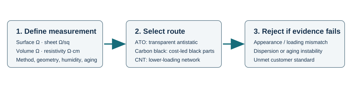
For transparent antistatic coatings, start with ATO. For black conductive plastics and ESD compounds, start with conductive carbon black when cost dominates, and CNT routes when lower loading or better conductivity efficiency justifies the premium. For 2D or anisotropic networks, compare graphene nanoplatelet (GNP) and MXene only after dispersion, orientation, sedimentation, oxidation, and aging risks are controlled.
What Are Material ESD?
ESD-control materials adjust surface resistance, volume resistance, charge-generation behavior, or charge-decay performance in plastics, coatings, films, adhesives, packaging, and handling components. Finished systems must still be validated for appearance, mechanical performance, and environmental durability.
Mekanisme
Controlled charge transport through a surface or bulk pathway, which may arise from a percolating filler network, interparticle tunneling, a continuous conductive coating, or surface ionic conduction.
The mechanism depends on the following system interfaces:
- matrix or binder interface
- substrate or part geometry
- processing shear window
- filler morphology, aspect ratio, orientation, and spacing
- film or part thickness
- contact and grounding configuration
- test voltage and electrode geometry
- humidity and aging environment
Pemilihan material
Read each row as a scenario-specific route: the guidance explains why a material fits, while the rejection boundary shows when to stop screening it.
Wide table — scroll horizontally to review every selection and rejection field.
| Scenario | Materials | Guidance |
|---|---|---|
| Transparent or light-color ESD coatings and films | ATO | Start with ATO when visible transmission, low color impact, or a light-colored appearance is required and moderate conductive performance is sufficient. |
| Black ESD plastics, trays, and packaging | MWCNT / FWCNT Dispersion / GNP hybrid | Evaluate multi-walled carbon nanotubes (MWCNT), few-walled carbon nanotube (FWCNT) dispersions, and CNT/GNP blends when black appearance is acceptable; optimize loading and dispersion against resistance, melt viscosity, impact properties, elongation, and molding quality. |
| Lowest loading conductive network | SWCNT | Evaluate well-dispersed SWCNT when very low loading or a very thin conductive network is required. Consider SWCNT-nano-Ag only where comparative data demonstrate an advantage over unmodified SWCNT. |
| Thin conductive films or advanced coatings | MXene / SWCNT / Ionic-Liquid Exfoliated Graphene | Compare SWCNT, graphene-based, and MXene-based routes according to conductivity, transparency, flexibility, coating process, and environmental stability; validate aging, residual ions, moisture sensitivity, and batch consistency. |
| Avoid these mismatches | ATO / MWCNT / SWCNT / MXene / GNP | ATO is usually not the first choice for the lowest-resistance opaque compound when carbon fillers are acceptable; avoid MWCNT/GNP/FWCNT for transparent layers; avoid SWCNT, SWCNT-nano-Ag, or MXene when packaging cost or long-term stability validation dominates. |
Scope Boundary
- ESD control is not equivalent to EMI shielding or current-carrying conductivity; it targets charge generation, accumulation, decay, and discharge under a specified test method.
- Do not use ESD material guidance as proof of EMI shielding or power-conductor performance; static-dissipative resistance is a different design target.
Scenarios and Subtypes
Use the host-system or subtype constraint to narrow the material direction before comparing grades or supplier data.
Scroll horizontally to review every scenario field.
| Scenario | Key constraint | Material direction |
|---|---|---|
| Coatings | Confirm surface resistance after leveling, adhesion, abrasion, and humidity exposure. | ATO, MWCNT, SWCNT, MXene, or graphene selected by transparency, loading, and coating thickness. |
| Plastics / compounds | Confirm volume resistance without excessive viscosity, brittleness, or molding defects. | Screen conductive carbon black, MWCNT, or carbon hybrids for practical ESD parts; consider SWCNT particularly when low loading, thin walls, or restricted viscosity increase justify its qualification cost. |
| Films | Confirm surface resistance or voltage decay with thin-layer continuity, haze, and flexibility limits. | ATO and other TCO routes are candidates for transparent or light-colored films; low-coat-weight SWCNT and selected graphene networks may also be transparent-to-translucent. MXene needs oxidation and humidity validation. |
| Adhesives | Confirm volume resistance after cure, aging, and bondline movement. | Screen conductive carbon black, MWCNT, GNP, or hybrid carbon systems by bondline thickness, viscosity, cure chemistry, and target resistance. Treat MXene as an advanced option requiring storage, cure, and aging validation. |
| Packaging and handling trays | Confirm charge decay or surface resistance after abrasion and handling exposure. | Screen conductive carbon black, MWCNT, permanent polymeric antistatic, or hybrid routes for resistance, charge generation, cleanliness, abrasion, and permanent versus migratory behavior. |
Resistance and Testing Requirements
Confirm the resistance method, charge-decay target, conditioning environment, and durability exposure before selecting a material.
Scroll horizontally to review every resistance and testing field.
| Target type | Reference band | Note |
|---|---|---|
| Surface resistance / sheet resistance for coatings, films, and ESD layers | Report exactly as the method specifies: Ω for surface resistance; Ω/sq for sheet resistance or surface resistivity. Include electrode geometry, humidity, voltage/time, thickness, substrate, and aging state. | Use ATO for transparent or light-color antistatic targets; use carbon black or CNT routes for black lower-resistance targets. Confirm the customer standard before claiming dissipative or conductive performance. |
| Volume resistance / volume resistivity for filled plastics and compounds | Report Ω for volume resistance or Ω·cm for volume resistivity, including molded direction, specimen geometry, filler loading, humidity conditioning, and post-processing state. | Use CNT routes when lower loading and conductivity efficiency matter; use conductive carbon black when cost and robust availability dominate. Evaluate GNP, MXene, and hybrid routes only with dispersion and aging data. |
Mode kegagalan
Use failure rows to identify a measurable trigger and the corresponding design response.
Wide table — scroll horizontally to review causes, signals, and responses.
| Failure type | Root cause | Manifestation | Mitigation strategy |
|---|---|---|---|
| Resistance Drift | Humidity sensitivity, additive migration, binder aging, or damage to the conductive network. | Resistance shifts after humidity, aging, abrasion, or handling exposure. | Improve filler-binder compatibility, reduce additive migration, stabilize filler spacing, optimize crosslink density, or select a more environmentally stable conductive system. |
| Agglomeration | Poor wet-out, incompatible resin polarity, high aspect-ratio entanglement, or insufficient dispersion energy. | Specks, surface defects, haze, uneven resistance, or batch-to-batch conductivity variation. | Use a compatible dispersion package, surface treatment, staged letdown, or a more readily dispersible filler where increased percolation loading is acceptable. |
| Poor Durability | Weak adhesion, exposed filler, coating-stack mismatch, or abrasion-sensitive conductive pathway. | ESD performance drops after abrasion, tape pull, handling, or thermal-humidity aging. | Improve adhesion package, change binder chemistry, reduce exposed filler, or select a more durable conductive network. |
| Low-Charging Failure | Material pairing, surface chemistry, contamination, humidity, motion, or contact area produces charge independently of the measured resistance. | Generated charge or surface voltage exceeds customer acceptance while resistance remains inside the specified band. | Test the actual material pairing and handling motion; adjust surface chemistry, contact, grounding, humidity control, or the material route according to the applicable customer method. |
Data validasi yang diminta
Scroll horizontally if the requested measurement text extends beyond the viewport.
| Measurement requested |
|---|
| Surface resistance after humidity aging under the customer electrode geometry and conditioning method. |
| Volume resistance in the final compound, adhesive, film, coating, or molded geometry when bulk dissipation is required. |
| Charge decay or voltage decay testing under the specified ESD program method. |
| Triboelectric charge generation or low-charging behavior under the defined material pairing, contact-and-separation motion, humidity, grounding, and handling conditions; do not infer it from resistance or resistivity. |
| Resistance uniformity mapping after processing, abrasion, handling, storage, and thermal-humidity exposure. |
| Dispersion, haze, color, viscosity, adhesion, and mechanical retention data at the selected additive loading. |
Test Methods and Reporting
Wide table — scroll horizontally to review methods and acceptance signals.
| Test method | Metode | Acceptance signal |
|---|---|---|
| Resistance-band confirmation | Measure surface resistance, volume resistance, charge decay, or voltage decay using the customer electrode geometry, humidity conditioning, final part geometry, and target ESD program method. | Candidate stays inside the antistatic, static-dissipative, or conductive band with acceptable uniformity across the part or coating. |
| Appearance and process window | Record haze, transmission, color, viscosity, loading, dispersion microscopy, leveling, coating defects, molding behavior, adhesion, and mechanical retention at the proposed additive level. | Candidate meets the electrical target without breaking transparency, color, viscosity, mechanical, or process limits. |
| Durability and drift screen | Recheck resistance after humidity aging, thermal cycling, abrasion, handling, cleaning, storage, and retained-sample batch comparison. | Resistance drift, charge-decay change, adhesion loss, abrasion damage, and network disruption remain inside customer acceptance. |
| Low-charging behavior | Measure charge generation, surface voltage, or charge decay for the actual material pair under the specified contact-and-separation motion, conditioning, handling, and grounding arrangement. | Generated charge and retained voltage stay inside customer acceptance independently of whether resistance meets its specified band. |
Technical Basis & References
Use the customer-specified method and keep each standard inside its scope. ANSI/ESD STM11.11, ANSI/ESD STM11.12, and IEC 61340-2-3 address resistance measurements relevant to ESD-control materials; IEC 62631-3-1 and IEC 62631-3-2 address DC volume and surface resistance or resistivity of electrical insulating materials. ANSI/ESD S541 and IEC 61340-5-3 define packaging requirements, while ANSI/ESD S20.20 and IEC 61340-5-1 define ESD control programs rather than material test methods. Use ASTM D257 only when its insulating-material scope fits the specimen; it is not the default method for moderately conductive materials. Treat withdrawn IEC 60093 only as a legacy customer-specified reference. Report the metric, unit, conditioning, electrode geometry, specimen thickness, grounding configuration, aging state, measurement voltage, and electrification time.
- ANSI/ESD STM11.11-2022 — Surface Resistance Measurement of Planar Materials EOS/ESD Association, Inc. · 2022
Defines reproducible surface-resistance measurement procedures, equipment, sample preparation, and conditioning for planar materials.
- ANSI/ESD STM11.12-2021 — Volume Resistance Measurement of Planar Materials EOS/ESD Association, Inc. · 2021
Defines volume-resistance measurement and reporting for planar materials under specified preparation and conditioning.
- IEC 61340-2-3:2016 — Resistance and Resistivity of Solid ESD-Control Materials International Electrotechnical Commission · 2016
Covers resistance and resistivity methods for solid materials used to avoid electrostatic charge accumulation.
- IEC 62631-3-1:2023 — Volume Resistance and Volume Resistivity International Electrotechnical Commission · 2023
Defines a DC method for volume resistance and volume resistivity of solid electrical insulating materials.
- IEC 62631-3-2:2023 — Surface Resistance and Surface Resistivity International Electrotechnical Commission · 2023
Defines DC methods for surface resistance and surface resistivity of solid electrical insulating materials.
- ANSI/ESD S541-2026 — ESD Protective Packaging Materials EOS/ESD Association, Inc. · 2026
Defines packaging properties and referenced test limits for protecting electrostatic-discharge-sensitive items.
- IEC 61340-5-3:2022 — ESD Protective Packaging Requirements International Electrotechnical Commission · 2022
Defines ESD protective packaging properties, classifications, referenced test methods, and performance limits.
- ANSI/ESD S20.20-2021 — ESD Control Program Requirements EOS/ESD Association, Inc. · 2021
Defines administrative and technical requirements for an organizational ESD control program; it is not a material test method.
- IEC 61340-5-1:2024 — ESD Control Program General Requirements International Electrotechnical Commission · 2024
Defines general requirements for establishing, implementing, and maintaining an ESD control program.
- ASTM D257-14(2021)e1 — DC Resistance of Insulating Materials ASTM International · 2021
Covers DC resistance and resistivity of insulating materials and states that moderately conductive materials require another applicable method.
- IEC 60093:1980 — Volume and Surface Resistivity of Solid Electrical Insulating Materials (Withdrawn) International Electrotechnical Commission · 1980 (withdrawn)
Official IEC lifecycle record identifies this legacy standard as withdrawn and replaced by IEC 62631-3-1 and IEC 62631-3-2.
FAQ
Should ESD plastics use MWCNT or SWCNT?
MWCNT is often the more established cost-performance route for black ESD compounds. Consider SWCNT when very low loading, thin walls, restricted viscosity increase, or specialized performance justifies its material and dispersion cost.
When should ATO be used instead of carbon additives?
Use ATO when transparency, haze, color, or light appearance is a key constraint. Use carbon additives when stronger conductivity, low loading, or black compound acceptance matters more.
What causes resistance drift in ESD materials?
Resistance drift can come from humidity, additive migration, thermal cycling, polymer relaxation, binder aging, abrasion, filler-network damage, or poor compatibility between the conductive additive and host system.
What information is needed for ESD project review?
Aurexene Materials needs the application area, required metric and test method, host resin or binder, process method, thickness, loading ceiling, grounding arrangement, optical or color limits, service environment, acceptance limits, sample quantity, and scale-up timeline.
Which material is best for cost-balanced ESD trays or packaging?
For black permanent ESD trays, conductive carbon black, MWCNT, and carbon-filler hybrids are common starting points. Select MWCNT/GNP hybrids only where comparative compound data show an advantage for the required resistance, cleanliness, mechanical properties, molding process, and filler loading.