
Application
Printed Electronics Inks & Conductive Pastes
Application guide for conductive inks and pastes used in printed circuits, sensors, electrodes, crossovers, and flexible electronic interfaces.
Quick Answer
Use Graphene Copper (Graphene-Cu) when a copper-assisted carbon interface is suitable, Single-Walled Carbon Nanotubes (SWCNT) for low-loading flexible networks, and Conductive Carbon Black for robust carbon ink or resistance-tuning routes; metal nanopowders remain gated until material review is complete.
What Are Printed Electronics Inks & Conductive Pastes?
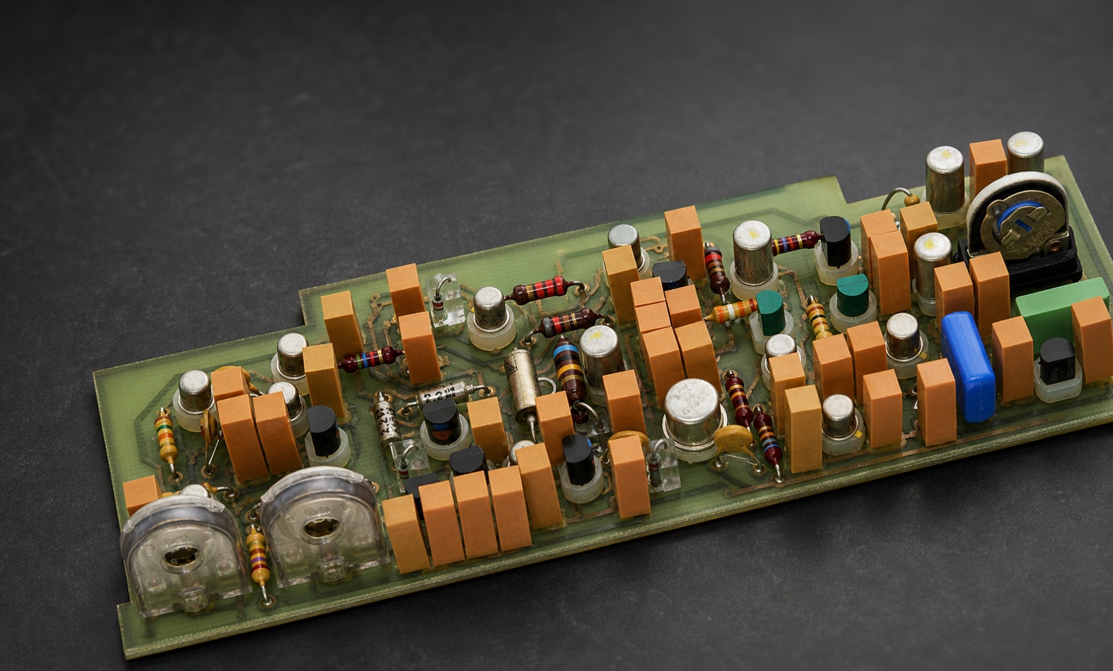
Printed-electronics inks and conductive pastes must form repeatable electrical paths through printing, drying or cure, bending, adhesion, and environmental aging on the selected substrate.

Mechanism
Carry current or define resistance while maintaining printable rheology, adhesion, geometry, and environmental reliability.
The mechanism depends on the following system interfaces:
- ink vehicle, substrate wetting, surface treatment, and cure adhesion
- screen, stencil, gravure, flexographic, aerosol, inkjet, or dispensing path
- contact pad, overprint, encapsulant, and assembly interface
Material Selection
Read each row as a scenario-specific route: the guidance explains why a material fits, while the rejection boundary shows when to stop screening it.
| Scenario | Materials | Guidance |
|---|---|---|
| Flexible low-loading printed network | SWCNT | Use SWCNT when thin, flexible conductive paths justify tight dispersion, filtration, and print-uniformity control. |
| Copper-assisted conductive paste or interface | Graphene-Cu | Use Graphene-Cu when contact performance can be balanced with copper oxidation, migration, cure, and storage controls. |
| Carbon ink and resistance tuning | Conductive Carbon Black | Use conductive carbon black when black appearance is acceptable and particulate loading remains inside viscosity, print, and adhesion limits. |
| Metal nanopowder printed-conductor route | Nano Ag Powder / Nano Cu Powder | Confirm exact-grade oxidation, migration, corrosion, cure, storage, and contact-resistance data before selecting a silver or copper nanopowder paste route. |
Scope Boundary
- Printed electronics is not conventional subtractive PCB fabrication; it forms functional electrical features by depositing printable inks or pastes.
- Do not use this route for conventional bulk wiring or PCB copper features when no printable, coatable, or low-temperature deposited conductive layer is required.
Scenarios and Subtypes
Use the host-system or subtype constraint to narrow the material direction before comparing grades or supplier data.
| Scenario | Key constraint | Material direction |
|---|---|---|
| Screen-printed circuits and crossovers | Mesh passage, line definition, dry thickness, cure, resistance, and substrate adhesion. | Graphene-Cu, SWCNT, or Conductive Carbon Black by resistance and appearance. |
| Flexible sensors and electrodes | Bending retention, surface uniformity, contact design, and environmental stability. | SWCNT-led network or carbon ink route. |
| Conductive interface pastes | Contact resistance, cure temperature, oxidation, migration, corrosion, and joint reliability. | Graphene-Cu after interface and environmental qualification. |
Target Performance Bands
Compare printed resistance together with line geometry, dry thickness, substrate, vehicle, print method, cure, adhesion, flexing, aging, and storage stability.
| Metric | Target range | Unit | Condition | Required |
|---|---|---|---|---|
| Printed conductor resistance | Customer-defined sheet, line, or contact resistance at final dry thickness. | ohm/sq, ohm/cm, mΩ, Ω, µm dry thickness | Final substrate, cure, geometry, and electrode configuration. | yes |
| Printability and line quality | Stable passage, leveling, edge definition, coverage, and defect rate under the production print method. | Pa·s, mPa·s, solids %, mesh/nozzle µm, line width µm, edge roughness µm, defect count | Actual mesh, nozzle, squeegee, speed, temperature, and ink age. | yes |
| Adhesion and flex retention | Resistance and adhesion remain inside acceptance after bend, abrasion, stretch, fatigue, and assembly handling. | adhesion rating, bend radius mm, cycles, abrasion cycles, elongation %, Δresistance % | Final substrate, overprint/encapsulant, bend geometry, abrasion method, and assembly stack. | yes |
| Oxidation, migration, corrosion, and storage stability | Resistance, leakage, viscosity, physical integrity, and contact performance remain inside acceptance after storage and environmental exposure. | hours, °C/%RH, bias V, Δresistance %, migration distance µm, viscosity drift % | Metal content, vehicle, encapsulation, voltage bias, humidity, temperature, cleaning media, and storage condition. | yes |
Failure Modes
Use failure rows to identify a measurable trigger and the corresponding design response.
| Failure type | Root cause | Manifestation | Mitigation strategy |
|---|---|---|---|
| Printed resistance is too high or nonuniform | The conductive network did not survive printing and drying as a continuous path. | Resistance map variation, open lines, edge defects, or agglomerates. | Adjust material route, dispersion, solids, print settings, thickness, and cure. |
| Adhesion or flex failure | The conductor cannot accommodate strain or maintain substrate contact. | Cracking, delamination, resistance jumps, or visible wear after bending or abrasion. | Change binder, surface treatment, filler architecture, thickness, cure, or encapsulation. |
| Resistance drifts during storage or environmental exposure | Material chemistry or interface protection is incompatible with the environment. | Rising resistance, leakage, discoloration, corrosion products, or storage viscosity drift. | Add protection, change chemistry, tighten storage, or select a more stable route. |
Validation Data Requested
| Measurement requested |
|---|
| Ink solids, viscosity, particle or network distribution, storage stability, and filtration data. |
| Print passage, line definition, dry thickness, coverage, surface roughness, and defect map. |
| Sheet, line, and contact resistance before and after cure and assembly. |
| Adhesion, bend, abrasion, stretch, and fatigue-retention data. |
| Humidity, thermal cycling, oxidation, migration, corrosion, cleaning-media, and storage exposure data. |
FAQ
Which material should be screened first for flexible printed electronics?
Start with the required resistance, feature size, substrate, cure, and bend profile; SWCNT is a low-loading option when the process can preserve its network.
When is Graphene-Cu appropriate?
Use it for copper-assisted contact or paste studies only when oxidation, migration, corrosion, storage, and cure can be qualified.
Can conductive carbon black be used for fine printed features?
It can be screened, but loading, roughness, binder demand, viscosity, and line definition may limit small features.
Are nano Ag, Cu, Ni, and Sn included in this draft?
Nano Ag and Nano Cu are review-gated candidates for printed-conductor studies; do not recommend them publicly until oxidation, migration, corrosion, storage, cure, and contact-resistance data are approved.
What data is needed before scaling an ink?
Provide substrate, print hardware, geometry, dry thickness, vehicle, solids, viscosity, cure, resistance, adhesion, and aging requirements.